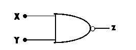
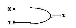
Concept:The logic gate shown in Figure 2 is identified by its standard circuit symbol.Explanation:The symbol in Figure 2 is an AND gate with a small circle (bubble) at its output.This bubble represents a NOT operation.An AND gate followed by a NOT gate is called a NAND gate.Therefore, the gate performs the NAND operation, giving an output of 0 only when all inputs are 1.